Usefull datas:
Moreover, you will remove the original ram chip! If you manage not to loose the memory, you are not born on this planet!!
|
 |
 |
| Before | After |

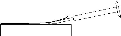
Believe it or not, these rivets aren't all that critical to holding
the unit together, so you can be as careful or as reckless as
you want (I prefer reckless, because I hate plastic rivets). A
good way to carefully remove the rivet heads is to use a flat
head screwdriver that is the same width as the recessed rivet
hole (4mm?) and "drill" the head away by hand with the screwdriver.
(I used a real drill to do this operation - SG).
 |
|
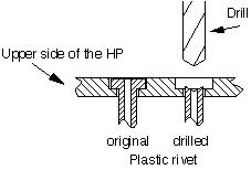 |
The head is about 2mm deep, so stop "drilling" there to leave
the keyboard material shoulder intact for easier reconnection
later. There are 6 rivets near the number keys and four above
the screen. These rivets above the screen perform more of a holding
function than the others, and you may want to consider using some
screws and small washers to replace them when you re-assemble.
 This is a close-up of a drilled rivet.
The only obstacle is the snap-together "hooks" that David Holmes refers to. These hooks are positioned near the [A], [F], [SIN], [1/x], [ON], [+] and [.] keys (the one by the [.] key is a real bugger!). Refer to the cutaway diagram below for details.
Key overlay here ___
                    \     ____________
                     \   |            |
             ____________|    ______  |
                             |   _  | |  <--- Upper section.
                             |  | | | |
             ________________|  | | |_|
                             |  | |___
  Circuit board and other    |  |     |
  components (affixed to     | /      |  <--- Lower section.
  upper section)             |/__     |        Has a lip which
                             |   |    |        engages with metal
           Metal "hook" ---> | / |    |        "hook" from upper
                             |/  |    |        section.
                             |   |    |
             ________________|   |    |
                                 |    |
To separate the two sections, you will need to push the lower
section out and down around the hooks. You can't do this from
the outside because the upper section hangs over the lower, so
you have to go from the inside. Luckily, the six slots in the
keyboard (used by the separate user-overlays that fit over the
original overlay) near the [MTH], [ENTER], [blushift], [NXT],
[backspace] and [-], come in handy for this. These slots are not
exactly lined up with the hooks, but are close enough. You can
insert something in these holes (I used a jewelers screwdriver,
flat head) at an angle that is mostly down and somewhat out, to
a depth of about 5mm, and come in contact with the lower section.
Push the lower section out about 2mm (this will take a bit of
force), while wedging something in the outside gap to separate
and hold the sections apart while working on the other hook positions
( a wooden matchstick works). I recommend starting with the [A]
or [F] positions first, working down whichever side you started
with, then do the other side, and leave the [.] position for later
(there is no helpful slot there).
 |
 |
| The two battery contacts which come through the case will need to go back through the case when the sections separate. The upper contact is hooked on a plastic boss, and needs to be freed from it. Just pop it off with your finger or a screwdriver. |  |
If you want to disassemble the unit further, like removing the circuit board from the upper section, you have a considerably tougher job on your hands, and you're on your own. Also, if you separate the screen from it's circuit board, you will disturb the rubber conductors (there are two) which provide electrical connection to the lcd rows and columns (zebra strips). Upon reassembly of the screen, you may find that you have lost some rows or columns in the display (not permanent, just a zebra strip alignment problem) and will have to keep reassembling and perhaps cleaning until it comes out okay. I haven't done this to my hp (yet) but I have done it to other cheap calculators and it wasn't fun.
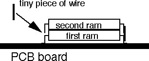
The ram chip is the original 32k ram. You can see on the left
the four pads waiting for the new 128k ram chip! The PCB of the
48G is the same as the 48GX! It differs only in the fact that
in the G ther's missing some chips. Especially the 74HC00 (bottom
of the picture) used to manage the port 1, and the 74HC174 used
for the bank switching mechanism used at port 2.
The Coil is used to generate regulated 5V (for the chips) and +/- 12V (for serial IO) from the 4.5 V delivered by the 3 batteries.The black capacitor maintain the ram while you are removing the batteries. You will also find there a good +5V source.
Port 1 is on the right, port 2 on the left (for the pins that are not the same for the two ports).
The CPU's name is Saturn. A nice processor with 64 bits internal registers, but with a data bus of 4 bits!!!
| You must desolder the original 32K ram chip. I used a needle
to bent up the pins while I was heating with the soldering iron.
As you can see, the RAM chip is the left one (the LCD display
being up and the battery case down). There is 28 pins to desolder.
We don't need this chip any more, so you can throw it if you want. Once this is done, check the absence of soldering bridges. Put some fresh solder on all the pins (there must be 32 pins, the first 28 used by the old ram, and the last 4 wich were free), it will be easier to solder the new ram. |
 |
 |
Solder the new ram, 128K x 8bits static SMD. Take care at the
orientation of the ram: The first pin is down near the ROM chip, near the battery case. There's a dot on the
chip near one corner of the ram locating the pin number 1. It allready works!! Close the HP (see how to do it) replace the batteries and check if the HP turns ON... If it doesn't, then you are in troubles... Reopen your HP, check all your solders, check for soldering bridges, try to bend up the pins to check if they are good soldered,... If you have done it carrefully, there should be no problems. At this point, you have 128K. You may want to stop now, there's no problem. If on the other hand you are brave enough, you can try to do the second part of the upgrade: adding 128k more for a total of 256k! |
All the pins have to be soldered on the first RAM except 3 of them: You have to bend up pins # 22, 24 and 30. They have
to be connected to some signals present at the place where the
card connector is usually soldered.
Take a look at the layout of the card connector and also at the pinout of the rams.
The pins 2,21,37,38 and 39 of the card connector are devided
for the two card slots. For all those pins you have to use only
the row of pins that has more distance from the battery case.
This is the row for card slot 1.
 pin 22:  connect it to pin 40 of the connector
 pin 24:     "            " 22           "
 pin 30:     "            " 21           "
There's some additionnal connections to do :
 the same picture at high resolution (232k)
Put now some adhesive tape on the metal shield to prevent shortcuts when you'll close the HP. Close the HP, and ready for the first test!
Reassembly-
Putting it back together is much easier. You may need to clean
up the remains of the rivet heads so they will easily reinsert
into their holes. Make sure the battery connections align with
their respective holes, and snap the unit together, applying pressure
where the six (or seven, if you left that one near the [.] key
alone) hooks are. 
You will probably want to hold the case together at the top with
one or two of the rivets there. If you can find a wood screw with
a flat or thin head, you can screw it into the body of the rivet
and let the head hold the upper section surface. You may need
a small washer for this. A machine screw will probably work as
well, but will strip the plastic easier and not hold as well.
I have only one screw holding mine together and it works fine.
You will probably need to re-shape your tin overlay, as it probably
took a beating during removal. I removed the sticky tape from
mine, but it's probably better not to (unless it really wont stick
anymore). Put wax paper over the tape and put the overlay face
down on a hard cover book. Grab a hammer with a smooth and somewhat
flat head, and pound away. DONT pound away on the part that surrounds
the screen (beveled part). You can probably use your fingers and
a little massaging to fix that area. With a little care you can
end up with an overlay that looks like new. Press the overlay
in place and hope it sticks. If not, a little rubber cement wouldn't
hurt.
Have fun!
Paul Smith
|
|||
To get rid of the "Invalid card data" message, type PINIT, or
just start using the port.
I wish everybody good luck on doing the upgrade !
 |
 |
| There's now 256K of ram! | "You know what? I'm happy..." On the left: Jean-Marc (the pictures are his HP) On the right: Myself |
                __                  __      __
     Vcc A15 CE2 WE  A13 A8  A9  A11 OE  A10 CE1 D8  D7  D6  D5  D4
  ____I___I___I___I___I___I___I___I___I___I___I___I___I___I___I___I____
  I  32  31  30  29  28  27  26  25  24  23  22  21  20  19  18  17   I
  I                                                                   I
   \                                                                  I
    I                                                                 I
   /                                                                  I
  I   1   2   3   4   5   6   7   8   9  10  11  12  13  14  15  16   I
  I---I---I---I---I---I---I---I---I---I---I---I---I---I---I---I---I---I
     NC  A16 A14 A12 A7  A6  A5  A4  A3  A2  A1  A0  D1  D2  D3  Gnd
And this is for the built in 32K chip. In my G it's labeled M5M5256BFP
and is located just above the battery case (the left one of the
two chips located there before you inserted the HC00).
                 __                  __      __
             VCC WE  A13 A8  A9  A11 OE  A10 CE1 D8  D7  D6  D5  D4
           ___I___I___I___I___I___I___I___I___I___I___I___I___I___I____
           I  28  27  26  25  24  23  22  21  20  19  18  17  16  15  I
           I                                                          I
            \                                                         I
             I                                                        I
            /                                                         I
           I   1   2   3   4   5   6   7   8   9  10  11  12  13  14  I
           I- -I---I---I---I---I---I---I---I---I---I---I---I---I---I--I
              A14 A12 A7  A6  A5  A4  A3  A2  A1  A0  D1  D2  D3  Gnd
As you can see the layout is nearly the same. Not for the pin
numbers but for the pin places if the chips are right assigned.Here is the 512k ram pinout:
         |-------\_/-------|
         |                 |
   A18 - | 1            32 | - Vcc
   A16 - | 2            31 | - A15
   A14 - | 3            30 | - A17
   A12 - | 4            29 | - Negative WE
    A7 - | 5            28 | - A13
    A6 - | 6            27 | - A8
    A5 - | 7            26 | - A9
    A4 - | 8            25 | - A11
    A3 - | 9            24 | - Negative OE
    A2 - | 10           23 | - A10
    A1 - | 11           22 | - Negative CS
    A0 - | 12           21 | - D7
    D0 - | 13           20 | - D6
    D1 - | 14           19 | - D5
    D2 - | 15           18 | - D4
   VSS - | 16           17 | - D3
         |                 |
|-----------------|PIN: Signal: PIN: Signal: 1 VCC (only if HP48 is ON) 21 Card enable (active HIGH) 2 RAM Battery measure 22 Output enable (active low) 3 Addr. 0 23 Data 1 4 Addr. 1 24 Data 2 5 Addr. 2 25 Data 3 6 Addr. 3 26 Data 4 7 Addr. 4 27 Data 5 8 Addr. 5 28 Data 6 9 Addr. 6 29 Data 7 10 Addr. 7 30 Data 8 11 Addr. 8 31 Video (port1) / EA 0 12 Addr. 9 32 Video (port1) / EA 1 13 Addr. 10 33 Video (port1) / EA 2 14 Addr. 11 34 Video (port1) / EA 3 15 Addr. 12 35 Video (port1) / EA 4 16 Addr. 13 36 Video (port1) / EA 5 17 Addr. 14 37 Write prot. in (act low) 18 Addr. 15 38 Card present in (act high) 19 Addr. 16 39 Card type (low for RAM) 20 Write enable (active low) 40 GroundNotes: